In the race to build more powerful AI systems, processor performance has surged ahead while memory bandwidth has struggled to keep pace. This growing disparity, often called the memory wall, threatens to leave even the most powerful AI chips starved for data. High Bandwidth Memory (HBM) is the technology designed to tear down that wall, and its importance has made it one of the most strategically valuable products in the entire semiconductor industry.
The Memory Bandwidth Problem
Modern AI workloads are extraordinarily memory-hungry. Training a large language model involves repeatedly reading and writing billions of parameters, and each training step requires moving enormous amounts of data between memory and compute units. Inference for these models requires the entire model's weights to be accessible in memory with minimal latency.
Traditional DRAM, connected to processors via a memory bus on a circuit board, cannot provide enough bandwidth for these workloads. A standard DDR5 memory channel delivers roughly 50 gigabytes per second. An AI processor like NVIDIA's H100 needs over 3,000 gigabytes per second, a 60-fold difference that no amount of DDR5 channels can practically bridge given the physical constraints of circuit board wiring.
HBM solves this problem through vertical integration. Instead of spreading memory across a circuit board, HBM stacks multiple DRAM dies directly on top of each other and connects them to the processor through a silicon interposer, providing a massively wide and short data path that delivers bandwidth impossible to achieve with conventional approaches.
How HBM Works
An HBM stack consists of multiple DRAM dies, typically 8 or 12, bonded vertically using through-silicon vias (TSVs). TSVs are tiny copper-filled holes drilled through each die that create vertical electrical connections between the stacked layers. Each die in the stack contains multiple independent channels, and the aggregate width of all channels across all dies provides enormous bandwidth.
The bottom of the HBM stack connects to a logic die (or buffer die) that manages the interface to the host processor. The entire stack is mounted on a silicon interposer alongside the processor die. The interposer contains a dense network of wires that connect the HBM stack to the processor with very short signal paths, typically just a few millimeters, minimizing latency and energy per bit transferred.
HBM Generations
HBM technology has evolved through several generations, each increasing bandwidth, capacity, and efficiency:
- HBM (2013): The original specification, offering 128GB/s per stack with four 2Gb dies. Used in AMD's Fiji GPU (Radeon R9 Fury).
- HBM2 (2016): Doubled bandwidth to 256GB/s per stack, with 8Gb dies. Used in NVIDIA's V100 GPU and AMD's MI50.
- HBM2E (2020): Extended HBM2 with higher speeds, reaching 460GB/s per stack. Used in NVIDIA's A100 GPU.
- HBM3 (2022): New architecture with per-die channels, reaching 819GB/s per stack. Used in NVIDIA's H100 and AMD's MI300X.
- HBM3E (2024): Enhanced HBM3 with higher speeds and 12-die stacks, reaching over 1.2TB/s per stack. Used in NVIDIA's H200 and B200 GPUs.
Each generation has roughly doubled the bandwidth of its predecessor while increasing capacity. The progression from four-die to eight-die to twelve-die stacks has been enabled by advances in TSV manufacturing and wafer thinning, which allows each die to be ground down to just 30-40 micrometers thick.
Why AI Needs HBM
The relationship between AI performance and memory bandwidth is direct and measurable. For large language model inference, the primary bottleneck is reading model weights from memory. Each token generated by a model like GPT-4 or Claude requires reading through all of the model's parameters. The rate at which tokens can be generated is therefore directly proportional to memory bandwidth.
A concrete example: a 70-billion parameter model stored in FP16 precision occupies 140GB of memory. Generating a single token requires reading all 140GB of weights (simplified, but directionally correct). With HBM3 delivering 3.35TB/s across multiple stacks, the theoretical maximum generation speed is about 24 tokens per second. With DDR5 at 200GB/s (using multiple channels), the same model would generate fewer than 1.5 tokens per second.
For AI training, the calculation is more complex because training involves both reading weights and writing gradients, but the bandwidth dependency is similarly strong. HBM enables the high-throughput matrix multiplications that dominate training computation, keeping the processor's compute units fed with data rather than idling while waiting for memory.
The HBM Supply Chain
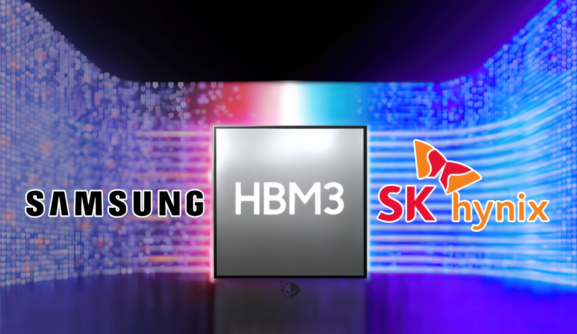
Only three companies manufacture HBM: SK hynix, Samsung, and Micron. This extreme concentration gives HBM production an outsized impact on the entire AI industry.
SK hynix: The Market Leader
SK hynix has dominated the HBM market, holding approximately 50% market share and enjoying first-mover advantage with each new generation. The company was first to qualify HBM3 and HBM3E with NVIDIA, its largest customer. SK hynix's HBM manufacturing is concentrated in South Korea, with expansion planned in the United States through a partnership with TSMC's Arizona fab for advanced packaging.
SK hynix's close relationship with NVIDIA is a significant competitive advantage. Being qualified as a primary supplier means SK hynix's HBM is designed into NVIDIA's products from the beginning, giving it the highest-volume and most profitable position in the market.
Samsung: Catching Up
Samsung, the world's largest memory chip manufacturer, initially fell behind SK hynix in HBM quality and production. Reports in 2023-2024 indicated that Samsung's HBM3 chips had higher heat output and lower yields than SK hynix's, leading NVIDIA to initially reject Samsung's HBM3 for its products. Samsung has since improved its manufacturing and has been qualified as a secondary supplier for NVIDIA's products.
Samsung's challenge illustrates an important point: HBM manufacturing is significantly more difficult than standard DRAM. The TSV process, wafer thinning, die bonding, and integration with a logic die require specialized equipment and expertise that do not directly transfer from commodity DRAM production. Samsung's struggles despite being the world's largest memory maker underscore this difficulty.
Micron: The American Supplier
Micron, the only American HBM manufacturer, has entered the HBM market with competitive products. Its HBM3E product has been qualified by NVIDIA and offers competitive bandwidth and power efficiency. Micron's strategic importance is amplified by U.S. government interest in domestic semiconductor supply chains. The company has received significant CHIPS Act funding to expand its domestic manufacturing capacity.
HBM Supply and Demand
The AI boom has created a dramatic supply-demand imbalance for HBM. Industry analysts estimate that HBM demand will grow from approximately $16 billion in 2023 to over $100 billion by 2027, driven almost entirely by AI accelerators. All three manufacturers are converting existing DRAM production lines to HBM and building new capacity, but the complexity and lower yields of HBM production mean that supply expansion takes years.
HBM commands a significant price premium over standard DRAM. While commodity DDR5 sells for a few dollars per gigabyte, HBM3E commands roughly $15-20 per gigabyte. This pricing reflects both the manufacturing complexity and the intense demand from AI chip makers. HBM has transformed the memory industry's economics, with SK hynix and Micron reporting record profits driven by HBM sales.
The Future of HBM
HBM4, expected to arrive around 2026, will bring further architectural changes. Reports indicate that HBM4 will use a wider interface (2,048 bits compared to 1,024 bits in HBM3) and may integrate the logic die more closely with the DRAM dies, potentially combining logic and memory functions on the same die. Samsung has proposed a 3D stacked architecture for HBM4 that could further increase bandwidth and capacity.
Beyond HBM4, research into compute-in-memory and processing-in-memory architectures aims to address the memory wall more fundamentally by performing computations directly within the memory array, eliminating the need to move data to a separate processor entirely. While these approaches remain in the research stage, they represent the logical endpoint of the trend that HBM began: bringing memory and compute as close together as physically possible.
For the foreseeable future, HBM remains indispensable for AI computing. Any organization building or purchasing AI infrastructure must account for HBM availability and pricing in their planning. The three HBM manufacturers hold an enviable position at the intersection of the most important technology trends in the world, and the strategic importance of their products will only grow as AI models continue to scale.