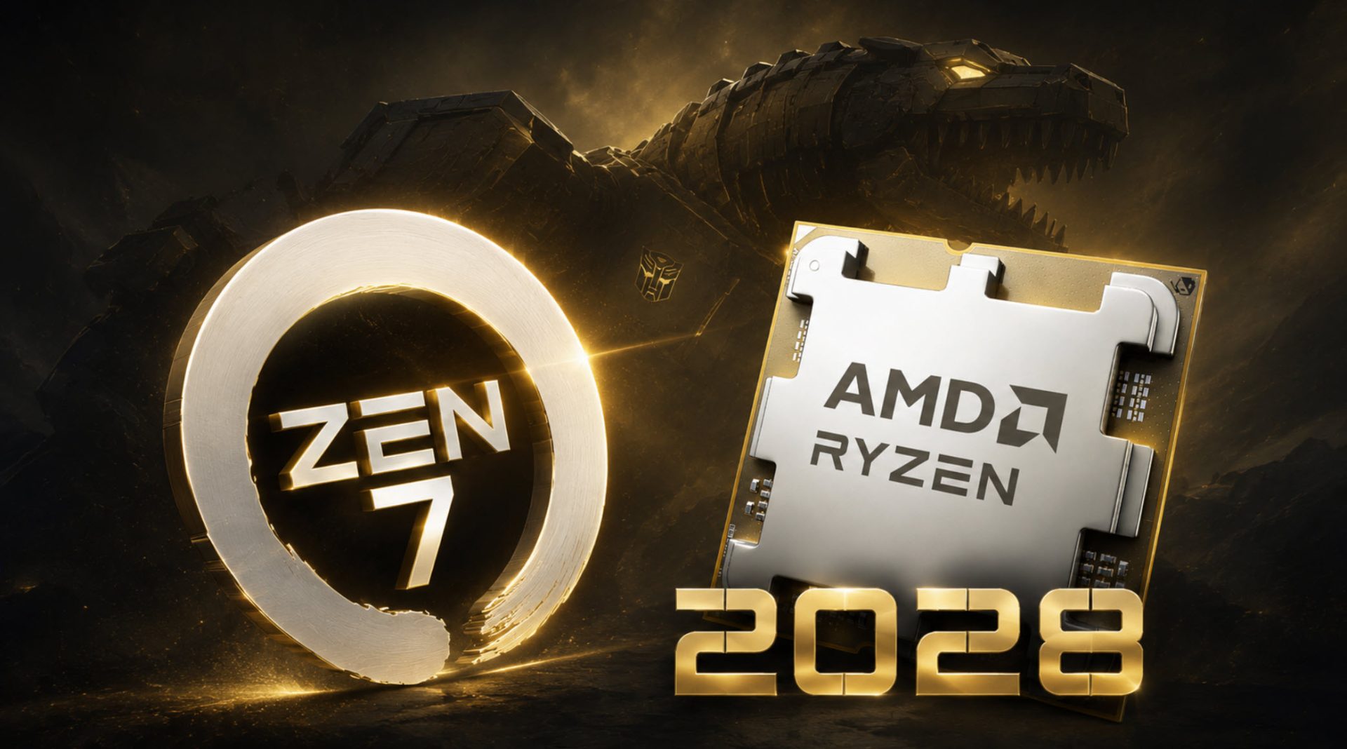
Everyone expected AMD to keep pushing incremental gains with its Zen architecture, perhaps a slight iteration on Zen 5 or a gradual rollout of Zen 6. But the silicon roadmap, as revealed by whispers from Taiwan’s Commercial Times, paints a far bolder picture. AMD’s upcoming Zen 7 CPUs, codenamed ‘Grimlock,’ are slated for a 2028 launch, banking on TSMC’s nascent 1.4nm (A14) process technology and potentially cutting-edge FOPLP packaging from Powertech. This isn’t just an update; it’s a strategic realignment, pushing the boundaries of what we thought was achievable for mainstream CPUs in the near-term.
What’s Really Under the Hood for Zen 7 ‘Grimlock’?
The details are still embryonic, but the reported integration of TSMC’s A14 process, a node that aims for the 1.4nm designation, is a significant signal. This isn’t merely about shrinking transistors; it’s about density, power efficiency, and raw performance that could redefine CPU capabilities. Coupled with this is the potential adoption of Fan-Out Panel-Level Packaging (FOPLP) from Powertech, a technology that allows for more complex and efficient integration of chiplets, potentially boosting cache and I/O capabilities. Think of it as building a more interconnected and powerful city on a smaller, more efficient footprint. This comes after AMD CEO Dr. Lisa Su’s recent visit to Taiwan, specifically to Powertech, adding a layer of credibility to the advanced packaging rumors.
AMD has begun its supply chain preparations for its next-generation Zen 7 platform ahead of schedule. Supply chain sources reveal that the Zen 7 core chipset (CCD), codenamed Grimlock, will utilize TSMC’s A14 process and incorporate next-generation 3D V-Cache technology.
The implications here are substantial. For consumers and enterprise users, this promises a leap in performance and efficiency. AMD’s Zen 7 is tipped to sport up to 16 cores per CCD, with a staggering potential of 224 MB of L3 cache on a single 3D V-Cache enabled chiplet. That’s not just an increase; it’s a doubling down on AMD’s cache-focused strategy, suggesting that the memory hierarchy will be paramount for unlocking future performance ceilings, particularly in data-intensive workloads.
Why Does This Matter for the CPU Wars?
The CPU market, once a duopoly, is now a three-way tussle, with AMD and Intel fiercely contesting the lucrative data center and AI markets dominated by NVIDIA. This push for 1.4nm and advanced packaging by 2028 isn’t just about competing with each other; it’s a race to keep pace with, or even preempt, the AI hardware juggernaut. With AI firms consuming CPUs at an unprecedented rate, every percentage point of performance gain, every watt of power saved, translates directly into billions of dollars. AMD’s aggressive roadmap for Zen 7 indicates a clear intent to remain a formidable player in this escalating battle, particularly in the $200 billion CPU TAM.
TSMC’s race towards A14 by 2028 is also a critical counter-move against Intel’s foundry ambitions. Intel has been making significant strides with its Intel 4, 3, and the upcoming 18A and 14A nodes, securing key customers like Apple and TeraFab. AMD’s commitment to TSMC’s A14 suggests a strategic choice to align with the foundry leader that has historically delivered superior yield and performance scaling. This dependency on TSMC, while seemingly safe, also represents a single point of failure for AMD’s bleeding-edge ambitions, a risk that becomes more pronounced as geopolitical tensions continue to simmer.
A Bet on the Long Game: Advanced Packaging’s Moment
What truly elevates this announcement beyond just another node shrink is the emphasis on advanced packaging. FOPLP, when fully realized, isn’t just about fitting more transistors; it’s about how those transistors communicate. It enables a modular approach, allowing AMD to mix and match different types of chiplets — compute, I/O, cache — with unprecedented efficiency. This flexibility is becoming increasingly vital as the limits of monolithic die scaling are tested. We’re not just building bigger chips; we’re building smarter, more interconnected systems on a package. This is the future, and AMD appears to be placing a significant bet on it, aiming to leapfrog competitors who might be slower to adopt these complex manufacturing and assembly techniques. It’s a bold, if somewhat audacious, play, but one that could define the next era of CPU design.
🧬 Related Insights
- Read more: VSORA’s Memory Wall Breakthrough: Can This French Upstart Reshape AI Inference?
- Read more: Zuck’s Tent Cities: How Meta’s $200M Talent Heist and GPU Bunkers Could Reshape AI for Everyone
Frequently Asked Questions
What is TSMC’s A14 process? TSMC’s A14 is their designation for a process technology targeting the 1.4nm node, aiming to deliver enhanced performance and power efficiency compared to current generations.
When will AMD’s Zen 7 ‘Grimlock’ CPUs be released? Current reports suggest a launch for Zen 7 ‘Grimlock’ CPUs in 2028.
What is FOPLP packaging? FOPLP stands for Fan-Out Panel-Level Packaging. It’s an advanced packaging technique that allows for more complex and integrated chiplet designs by enabling wider routing traces and denser connections on larger panel substrates.
Will this affect current CPU prices? While this announcement pertains to future products launching in 2028, significant advancements in manufacturing and packaging can eventually influence cost structures and market pricing over the long term as these technologies mature and become more widely adopted. The immediate impact on current CPU prices is unlikely.