Sanctions breed innovation.
That’s the oldest adage in the tech world, often bandied about with a knowing nod and a shrug. But Huawei, facing the full, unyielding weight of US export controls, isn’t just nodding. They’re building — and with astonishing density. Their new OceanDisk 1800 SSD, boasting a jaw-dropping 122.88TB of storage (with a 245TB model on the horizon), isn’t merely a proof to high-capacity storage; it’s a defiant declaration of architectural ingenuity, a direct response to being cut off from the global supply chain for advanced 3D NAND.
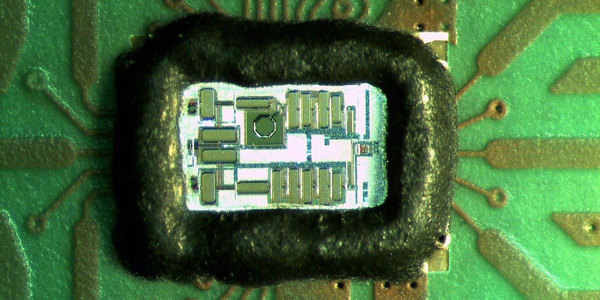
This isn’t about cramming more NAND dies into a familiar package. Huawei’s gambit involves a fundamental shift in how those dies are integrated: Die-on-Board (DoB) packaging. Forget the conventional BGA or TSOP packages; DoB means mounting the raw NAND flash chips directly onto the SSD’s printed circuit board (PCB). It’s a more intimate, less abstracted connection. Think of it less like plugging in a component and more like weaving threads directly into the fabric of the board itself. This approach circumvents the physical constraints and packaging limitations that typically cap the number of NAND dies in a given footprint.
The problem Huawei’s engineering brains needed to crack was simple, yet profound: the most advanced 3D NAND, with its dizzying number of stacked layers — we’re talking over 400 from outfits like Samsung — relies on American-origin technology. Even when produced by non-US companies, the underlying IP and manufacturing processes are often too intertwined with US tech to be legally supplied to Huawei. China’s own YMTC, while offering impressive 3D NAND, is currently capped at a less dense 232 layers. For a company aiming for the bleeding edge of data center and AI inference storage, that’s a significant bottleneck.
DoB ditches traditional NAND packaging and puts the NAND dies directly on the SSD’s PCB. This allows Huawei to increase the capacity of its storage devices while using YMTC’s less dense NAND dies.
By going DoB, Huawei essentially creates its own “stacking.” Instead of vertically layering silicon dies in their own neat, encapsulated packages, they’re laying them out side-by-side on the PCB, maximizing the available real estate. This isn’t just a clever workaround; it’s a statement about supply chain resilience and the potential for indigenous innovation when faced with extreme pressure. Of course, this architectural leap isn’t without its hurdles. Thermal management, always a beast in high-density storage, and maintaining pristine signal integrity across a board crowded with bare dies — these are not trivial engineering challenges. Huawei claims they’ve wrestled these demons into submission with the OceanDisk 1800.
The Geopolitical Undercurrents of Terabytes
It’s easy to get lost in the sheer scale of 122TB, to marvel at the engineering. But we can’t ignore the context. This isn’t just about enterprise storage; it’s a tangible manifestation of China’s drive for technological self-sufficiency. With Beijing actively restricting imports of high-end AI chips from the West — most notably, blocking Nvidia H200 models and even targeting consumer-grade GPUs like the RTX 5090D — Chinese firms are being nudged, or perhaps shoved, towards domestic solutions. Huawei’s DoB SSD directly feeds this ecosystem. It provides the storage backbone for local AI clusters, indirectly benefiting Chinese chipmakers who can then reinvest profits into R&D, further accelerating their journey toward decoupling from US technology. It’s a cycle, and one that Washington seems to be inadvertently fueling.
Is this the Future of High-Density Storage?
What’s particularly fascinating is how Huawei’s approach might influence the broader storage industry. While established players like Samsung and SK Hynix have been pushing the boundaries of multi-layer NAND stacking, Huawei is demonstrating that an alternative path exists. DoB packaging, with its direct-on-PCB integration, could offer a more cost-effective route to extreme capacities, especially if the advanced multi-layer stacking technologies remain off-limits or prohibitively expensive for certain markets. It also suggests a future where more custom silicon integration happens at the board level, blurring the lines between component and system design. This has implications not just for SSDs but for other complex hardware modules where density and cost are paramount.
While the immediate impact is felt in the data center and AI inference markets, the architectural shift Huawei has engineered with its 122TB SSD is a compelling case study. It’s a stark reminder that necessity, when coupled with deep engineering talent, can indeed be the mother of invention. The sanctions weren’t just an obstacle; they were a catalyst.
🧬 Related Insights
- Read more: Notebook Wars: Forget Specs, Your RAM Price Tag Decides Your Fate in 2026
- Read more: NVIDIA’s 007 GPU Giveaway: Marketing or Motivation?
Frequently Asked Questions
What is Die-on-Board (DoB) packaging? DoB packaging involves mounting bare NAND flash dies directly onto the SSD’s printed circuit board (PCB), bypassing traditional packaging methods like BGA or TSOP to increase density.
Can Huawei still buy advanced 3D NAND chips? No, due to US sanctions, Huawei is effectively blocked from acquiring high-layer-count 3D NAND chips that rely on American technology, even if produced by non-US companies.
Will this DoB technology be adopted by other companies? It’s possible. DoB offers a route to higher capacities and potentially lower costs, especially if advanced multi-layer NAND remains restricted or expensive for certain markets. It represents a significant architectural alternative.